A new strategy for advancing semiconductor performance beyond miniaturization
Today's highly information-driven society relies heavily on high-performance semiconductors. Generally, as semiconductor chips are miniaturized, their performance improves, so manufacturers have been devoting their energy to developing microfabrication technology for chips. However, further miniaturization is becoming increasingly difficult. This is due to the need for more advanced processing technologies, which lead to enormous investments in manufacturing equipment and reduced product yields, resulting in increased manufacturing costs.
As a new strategy to advance semiconductors’ performance, the technology of “chiplet integration” has gained attention. Instead of incorporating all necessary functions into a single chip, this approach involves creating chiplets (small chips) for each function and connecting them together to achieve the same functionality as a single chip. Smaller chiplets have better yields, and by selecting and connecting good-quality chiplets, the overall yield can be improved. Additionally, it is possible to focus on miniaturizing only the chiplets with critical functions, which is expected to help reduce manufacturing costs.
Packaging technologies suitable for chiplet integration
However, to integrate separately manufactured chiplets, innovative methods are required, and various approaches are being explored. One such approach is to use packaging technologies originally developed for single semiconductor chips. Semiconductor chips are always packaged to protect them from environmental damage and to establish electrical connections with printed circuit boards. The mainstream method for this is FOWLP (Fan-Out Wafer Level Package), which is also suitable for chiplet integration.
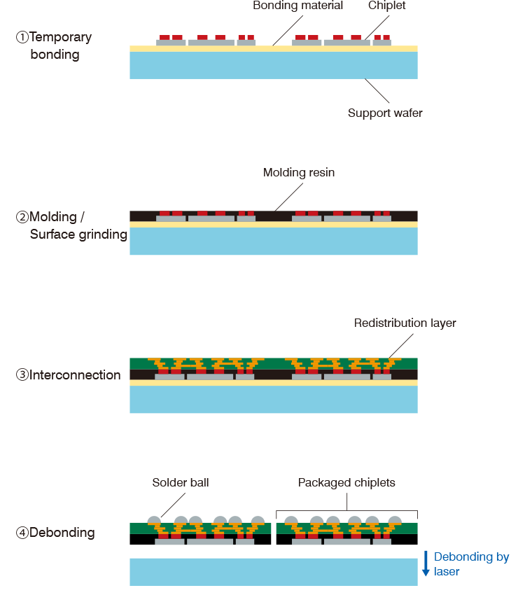
In FOWLP, the process is carried out on a translucent “support wafer.” The steps involved are as follows:
Step 1 Apply bonding material to the support wafer and temporarily fix the chiplets.
Step 2 Encapsulate the chiplet with molding resin and grind the surface to expose the electrode ends.
Step 3 Form redistribution layer.
Step 4 Use laser light to decompose the bonding material and debond the package from the support wafer.
FOWLP conducted on the support wafer
Ceramics for lighting lamps used as support wafers
Support wafers do not appear in the spotlight, but the performance required is strict. During the molding (step 2) and redistribution layer formation (step 3) processes, heat is applied to cure the resin, which can cause warpage due to the difference in thermal expansion coefficient between the resin and the substrate. This warpage needs to be minimized as much as possible, so the support wafer must have high rigidity. Additionally, in the debonding process (step 4), a laser is applied from the backside of the support wafer, so it must have high translucency. Furthermore, since the support wafer is cleaned with chemicals and reused multiple times, it must also be resistant to chemicals. Traditionally, glass has been used for support wafers, but its performance was insufficient.
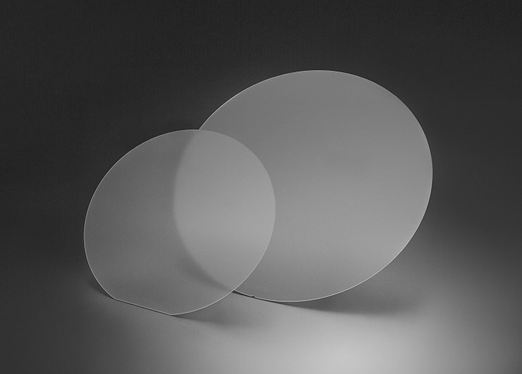
NGK has a ceramic material that meets the three properties required for support wafers. This is translucent alumina made from high-purity alumina, which has been used as a tube material for high intensity discharge lamps such as high-pressure sodium lamps and metal halide lamps from the 1980s until recently. NGK has evolved this ceramic material into a support wafer material, naming it HICERAM Carrier. However, since the FOWLP process uses the same equipment as for silicon wafer processing, the support wafer needs to be shaped to the same diameter (300 mm) and thickness (about 1 mm) as silicon wafers. NGK has achieved manufacturing at this size with its unique technology, enabling the packaging of many chiplet integrations at once. HICERAM Carrier is expected to support the advancement of high-performance semiconductors as a behind-the-scenes player.
HICERAM Carrier
Writer
Aoyama Seiko
Science and Technology Journalist
Aoyama Seiko studied chemistry at Ochanomizu University and its graduate school. She has worked in public relations for a research funding agency and as a journalist and editor for a chemistry magazine. She now works for Sci-Tech Communications, producing public relations materials (newsletters, website text, etc.) for research institutions and technology companies. She also teaches science writing at several universities.