High performance SAW filters essential for Beyond 5G
Smartphones have become a key part of modern society's infrastructure, and the development of technologies for the successor to the current 5G systems is accelerating. The next generation, known as Beyond 5G, will achieve high capacity, multiple simultaneous connections and ultra-low latency – communications that go beyond 5G.
In telecommunications, radio waves are divided into a large number of narrow channels, and a component known as the “SAW filter” is crucial. The SAW filter is about 1 mm square, and nearly 100 are installed in high-end smartphones. This device employs surface acoustic waves (SAW) propagating on a piezoelectric substrate, which expands and shrinks when voltage is applied, so that only radio waves of a specific frequency are transmitted. The frequency of the emitted radio waves is determined by the spacing between the electrodes, but as the temperature of the SAW filter rises during operation, the piezoelectric material expands thermally, causing the spacing between the electrodes to widen. As a result, the frequency of the radio waves passing the filter is shifted, and the communication quality is degraded because the noise cannot be cut properly.
NGK's bonded wafer realizes SAW filters that cause less frequency shift
NGK's bonded wafers are the solution to this problem. When SAW filters are made using bonded wafers with piezoelectric elements layered on a silicon base, the silicon, which is resistant to thermal expansion, suppresses the expansion of the piezoelectric elements, making it difficult for the electrode spacing to change and almost impossible for the frequency to shift.
More stable communication quality by reducing thermal expansion
![[conventional SAW filter] Piezoelectric material(thermally expands or shrinks easily) [NGK Bonded Wafer]Support substrate: Silicon(does not easily thermally expand or shrink)](img/kw8_item_img2.png)
Thermal expansion controlled down to 1/3 of conventional filter
To make this bonded wafer, the surfaces of both silicon wafer and piezoelectric wafer are activated, and the two are bonded together. The surface of the wafer is then precision polished to the desired thickness. The main advantage of this technology is that it allows for thin layers while maintaining the excellent performance of the piezoelectric material. Since the different materials are firmly and directly bonded at room temperature without using adhesives, the resulting bonded wafers are not distorted by thermal processing. The bonded wafer has high chemical resistance and can be processed with chemicals that would dissolve adhesives.
Optical communications devices can also be manufactured from bonded wafers
The bonded wafers can be made of various combinations of materials, not only piezoelectric (functional layer) and silicon (support substrate).
Beyond 5G is expected to require filters with higher performance than those for 5G. With bonded wafers, such filters can be fully realized. High-performance optical devices can also be manufactured from bonded wafers. These devices will be used at the entrance to optical communication networks connecting base stations for smartphones, and will contribute to speeding up communication between base stations.
Applications of NGK's bonded wafers expanding beyond communications
Applications of bonded wafers are expanding beyond telecommunications. One application is sensors – LiDAR technology, which uses lasers to detect objects, is indispensable in automatic driving in automobiles, and the optical sensors required for this technology can be made from bonded wafers. In the future, optical integrated circuits, which will be the core of quantum computers that use light, will also be realized by taking advantage of the characteristics of bonded wafers.
NGK's unique technology, which at first glance appears to be as simple as bonding different ceramics, is expected not only to support the era of “high-capacity, multiple simultaneous connection, and ultra-low latency” communications, but also contribute to realizing other advanced technologies.
Bonded wafer
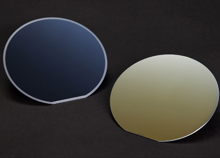
Bonded wafer for SAW filter (left) and bonded wafer using other piezoelectric materials
Writer
Aoyama Seiko
Science and Technology Journalist
Aoyama Seiko studied chemistry at Ochanomizu University and its graduate school. She has worked in public relations for a research funding agency and as a journalist and editor for a chemistry magazine. She now works for Sci-Tech Communications, producing public relations materials (newsletters, website text, etc.) for research institutions and technology companies. She also teaches science writing at several universities.