
Topics
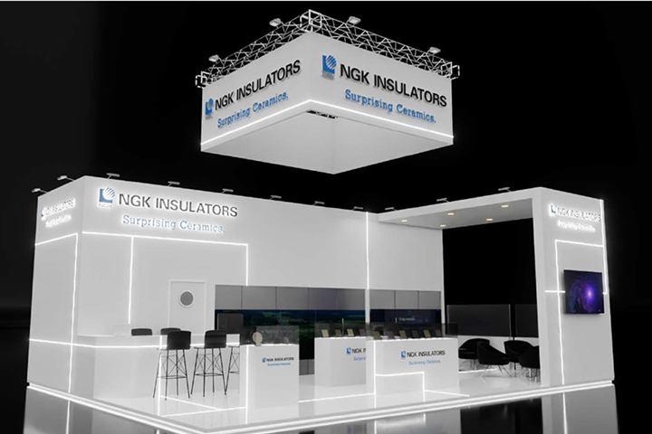
NGK is exhibiting at PCIM Europe 2024
June 05, 2024
NGK Insulators will exhibit at Power Conversion and Intelligent Motion: PCIM Europe 2024, Nuremberg, Germany from 11th to 13th June. PCIM is the one of the largest exhibitions, which is dedicated to the power electronics field, including power semiconductors, inverters and converters.
Outline of PCIM Europe 2024
| Dates | 11th (Tue.) to 13th (Thu.) June, 2024 |
|---|---|
| City / Country | Nuremberg, Germany |
| Venue | Nuremburg Messe |
| NGK Booth | Hall 9 - 404 |
| Official site | PCIM Europe |
Exhibition contents
SN-AMB/DCB Substrate
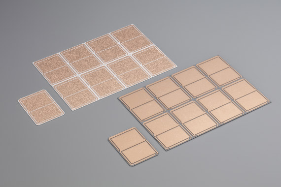
SN-AMB*1 and DCB*2 Substrates for Power Modules are products in which copper plates are bonded to each surfaces of a ceramic plate, which is an insulating material.
As ceramic materials, we offer silicone nitride-based materials and alumina-based materials, and a ceramic plate made of nitride-based material and that made of alumina-based material are integrated with copper plate through bonding by the active metal brazing (AMB) method and direct copper bonding (DCB) method, respectively. Those products are equipped with a high thermal conductivity and a high electric conductivity of copper and a high insulation property of ceramic substrate.
In the AMB method we conduct, a bonding layer with a thickness of several micron or less has been achieved, producing almost no influence of the thermal resistance of the bonding layer. In addition, in the DCB method, as a copper plate is directly bonded to an alumina-based ceramic substrate, there is almost no bonding layer that produces thermal resistance.
- *1SN-AMB: Si3N4-Active Metal Brazing method
- *2DCB: Direct Copper Bonding method
Product usage
Various power modules in which various power semiconductor elements, such as Si-IGBT and SiC-MOSFET, are mounted.
Power module units for electric vehicles, renewable energies (wind power, photovoltaic power generation, etc.), inverters for industrial uses.
AMB and DCB Substrates for Power Modules
SiC wafer (R&D Sample)
SiC wafers are the material for SiC power semiconductors, which are widely used in applications such as electric vehicles (EVs). The basal plane dislocation (BPD) density of SiC wafers is an important parameter for the performance of power semiconductors. NGK Insulators has developed a novel process that can reduce BPD density through simultaneous processing of multiple wafers, thus achieving a low cost. We will be exhibiting 6-inch SiC wafers grown using this process for the first time.
Large Current Ceramic Wiring Board (R&D Sample)
Large Current Ceramic Wiring Board is a new solution for wiring connections, which reduces switching surges and enables full-speed operation of SiC power devices by embedded thick Cu conductors in multi-layer ceramic substrate through NGK unique ceramic technologies.