
Topics
Exhibition at OFC2025
March 07, 2025
NGK Insulators (NGK) will participate in the International Conference on Optical Fiber Communications Conference and Exhibition (OFC) 2025, which will be held in San Francisco, California, United States, from Sunday, March 30, 2025, to Thursday, April 3, 2025. We will present our research findings on TFLN bonded wafer for optical communications. Additionally, we will exhibit related products, including our bonded wafer for optical communications and ceramic package.
Conference Overview
| Conference Name | Optical Fiber Communications Conference and Exhibition (OFC) 2025 |
|---|---|
| City / Country | San Francisco, California, United States |
| Venue | Moscone Center 747 Howard St, San Francisco, CA 94103 |
| NGK booth | Booth No. 6352 |
| Official Website | OFC |
| Dates | Conference: March 30 (Sun) to April 3 (Thu), 2025 Exhibition: April 1 (Tue) to April 3 (Thu), 2025 |
Presentation Overview
| Date and Time | April 3 (Thu), 2025, 10:15-10:45 |
|---|---|
| Room | Theater Ⅲ |
| Title | Introduction to NGK Bonded Wafer for Optical Communication |
| Presenters | Tomoyoshi Tai |
| Presentation Summary | We present our bonded wafer products, fabricated using direct bonding and high-precision polishing technology. These wafers are applied in various applications, including Thin-Film LiNbO3 (TFLN) photonic devices. With high crystallinity, uniform thickness, and exceptional stability, NGK’s wafers contribute to launching the new markets for optical communication applications. |
Exhibited Products
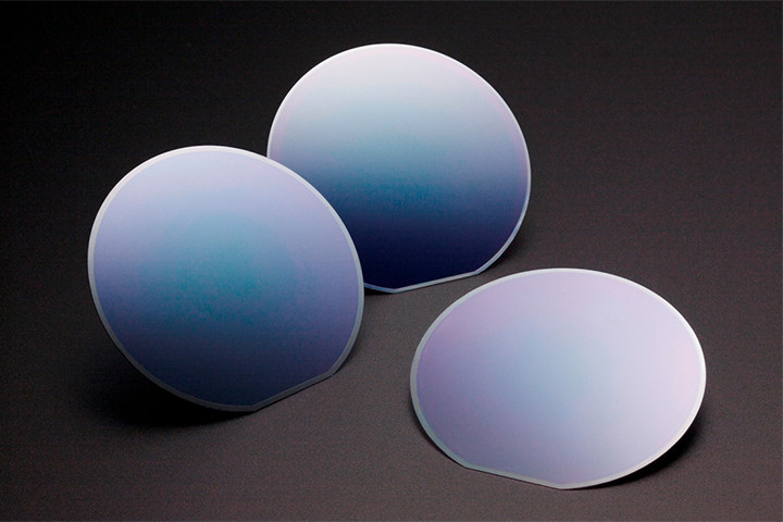
Bonded wafers
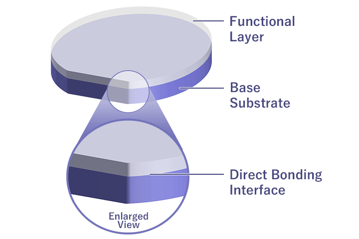
Bonded wafers are substrates for electronic devices fabricated by bonding together differing materials. The two types of substrates are directly bonded without using adhesive and then the functional layer undergoes ultra-precise thin polishing. This enables the addition of physical properties such as high insulation, high thermal conductivity, low thermal expansion, and high rigidity of the base substrate to improve various characteristics including temperature characteristics. Hybrid bonded wafers contribute to creating smaller, faster, and less power-consuming devices for applications such as filters for 5G communications, modulation devices for optical communications, sub-terahertz (sub-THz) antennas, and MEMS (Micro Electro Mechanical Systems) devices. NGK will display TFLN bonded wafer for optical communications, gallium nitride (GaN) wafers, and other items at this exhibition.
Wafer Products Product Site
TFLN bonded wafer for optical communications
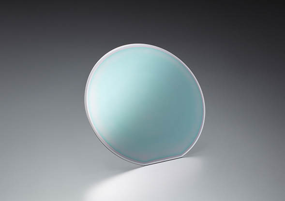
TFLN bonded wafers for optical communications are high-performance wafers made by precision-polishing a bonded wafer consisting of lithium niobate (LN) bonded to a base substrate. This product offers thin-film LNs free of crystal damage, which contributes to the development of optical modulation devices featuring lower power consumption and smaller dimensions—ideal for data centers and core/metro networks.
Gallium Nitride (GaN) Wafer
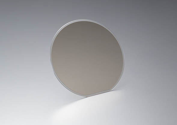
Our gallium nitride (GaN) wafers are high-quality GaN wafers with low dislocation density achieved using NGK's proprietary liquid phase crystal growth method.
We have developed two different types of GaN wafers: a semi-insulating type for high frequency devices for 5G and 6G wireless base stations; and a conductive type for the power devices incorporated into electric vehicles (EVs), power control units, and optical devices used as light sources for projectors.
The bonded semi-insulating GaN wafer exhibited at the exhibition, produced by combining a GaN thin film with a silicon carbide (SiC) base substrate, imparts the high heat dissipation properties of SiC to the low dislocation density GaN wafer, enhancing the performance and reducing the cost of high-frequency devices.
Gallium Nitride (GaN) Wafer
Ceramic Packages and Substrates
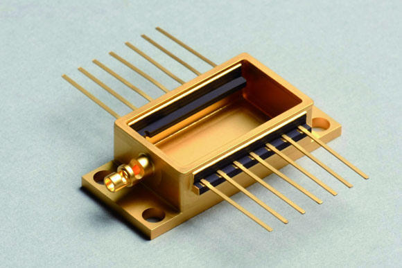
NGK’s ceramic packages and substrates support semiconductor devices in various forms used for 5G communication and beyond. The next-generation communication technology requires high-speed, large-capacity, low power, and low latency. NGK offers ceramic packages and substrates for RF power amplifiers, optical transceivers, and millimeter-wave communication which are essential to the next-generation communication infrastructure.
HTCC Product Site