
Creating new products
SiC Wafer That Improves Reliability and Lowers the Cost of Power Devices for Electric Vehicles
Overview of products under development
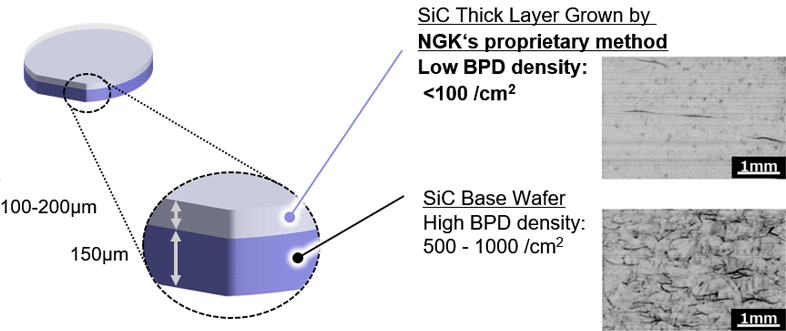
NGK has applied its proprietary crystal growth method to reduce basal plane dislocation (BPD) density, a critical defect found in silicon carbide (SiC) bulk wafers, paving the way to production of high-quality SiC wafers.
This new SiC wafer is expected to improve reliability and lower the cost of the power devices used in inverters for electric vehicles (EVs) and for other applications.
Properties
Higher reliability for SiC power devices
Drawing on proprietary crystal growth methods developed from its accumulated ceramic technologies, NGK is developing a SiC bulk wafer that features extremely low density of basal plane dislocations (BPD)—crystal defects that degrade performance in power devices. This suppresses bipolar degradation,* an issue encountered with power devices, and enables stable device performance for power devices even under high voltage and high current conditions.
Bipolar degradation: Bipolar degradation is a phenomenon in which basal plane dislocations (BPD) generated in SiC devices operating at high currents expand to create stacking faults, and increased on-resistance.
Improved yields, reducing the cost of SiC power devices
Our proprietary SiC bulk wafers, which exhibit low dislocation density, make it possible to achieve even lower dislocation density after epitaxial growth. This in turn improves yields for power devices and helps reduce costs.
Specification
| Parameters | Unit | Properties |
|---|---|---|
| Size | - | 4~6 inch (8 inch: Under development) |
| Polytype | - | 4H |
| Conductivity Type | - | Nitrogen / N-type |
| Surface Orientation | degree | 4 -off toward <11-20> ±0.5 |
| Resistivity | mΩ・cm | 15 - 25 |
| Micropipe Density | /cm2 | <1 |
| BPD Density | /cm2 | <100 |
Applications
SiC Wafers for Power Semiconductors
NGK is developing SiC wafers for power electronics applications that require high power, including inverters for electric vehicle (EV) motor control. We are also working on developing wafers of even larger diameters and higher quality and to rapidly establish mass production systems for these wafers.
Inquiry about Research & Developments
Please apply with the contact form and give us your comments or questions.