
Topics
Exhibition at EuMW2025
Bonded Wafers and GaN Wafers
for Wireless Communication Applications
September 17, 2025
NGK Insulators (NGK) will participate in the International Conference on European Microwave Week (EuMW) 2025, which will be held in Utrecht, the Netherlands, from Sunday, September 21, 2025, to Friday, September 26, 2025. EuMW is one of the largest international conferences and exhibitions in Europe focused on microwave, millimeter-wave, RF (radio frequency), and wireless communication technologies. We will present our quartz glass bonded wafers. Additionally, we will exhibit related products, including our bonded wafers for wireless communication applications and gallium nitride wafers.
Conference Overview
| Conference Name | European Microwave Week (EuMW) 2025 |
|---|---|
| City / Country | Utrecht, the Netherlands |
| Venue | Jaarbeurs Convention Centre Jaarbeursplein 6, 3521 AL Utrecht |
| NGK booth | Hall 7, Booth No. F137 |
| Official Website | EuMW |
| Dates | Conference: September 21 (Sun) to September 26 (Fri) Exhibition: September 23 (Tue) to September 25 (Thu) |
Presentation Overview
| Date and Time | September 24th (Wed), 2025, 10:50-12:30 (Poster session) |
|---|---|
| Room | Hall 7 |
| Title | Introduction of Quartz Glass Bonded Wafer for Sub-THz Antenna Circuits |
| Presenters | Kentaro Tani |
| Presentation Summary | This presentation introduces a cavity-structured quartz glass bonded wafer with a Fraunhofer Institutes*-designed antenna for D-band (140 GHz band) applications. The antenna achieves broadband operation with 13 dBi gain and 30 GHz bandwidth, making it suitable for high-resolution automotive in-cabin radar, such as vital sign and gesture sensing to enhance safety and comfort. |
- *Fraunhofer Institutes: Europe’s largest applied research organization headquartered in Germany.
Exhibited Products
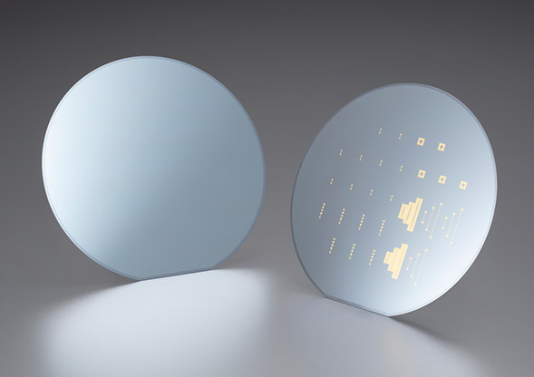
Bonded wafers
Bonded wafers are substrates for electronic devices fabricated by bonding together differing materials. The two types of substrates are directly bonded without using adhesive and then the functional layer undergoes ultra-precise thin polishing. This enables the addition of physical properties such as high insulation, high thermal conductivity, low thermal expansion, and high rigidity of the base substrate to improve various characteristics including temperature characteristics. Hybrid bonded wafers contribute to creating smaller, faster, and less power-consuming devices for applications such as filters for 5G communications, modulation devices for optical communications, sub-terahertz (sub-THz) antennas, and MEMS (Micro Electro Mechanical Systems) devices. NGK will display TFLN bonded wafer for optical communications, gallium nitride (GaN) wafers, and other items at this exhibition.
Wafer Products Product Site

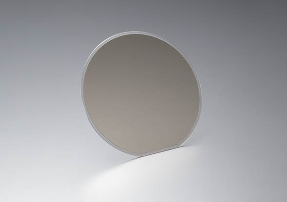
Quartz glass bonded wafers for sub-THz wireless communication
Quartz glass bonded wafers are manufactured by directly bonding quartz glass and silicon. Quartz glass provides low loss performance against sub-THz waves, and Si has relatively high heat dissipation properties. It contributes to the realization of antenna circuit boards with low loss, wide frequency bandwidth, high heat dissipation performance and high reliability for 6G communications and high frequency radar.
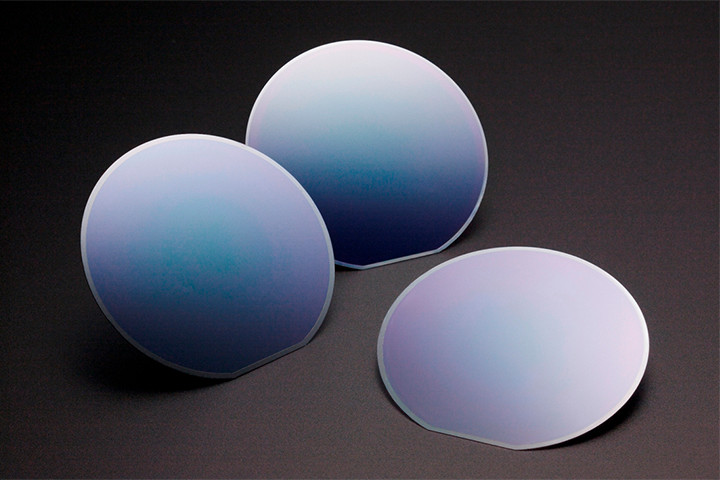
Gallium Nitride (GaN) Wafer
Our gallium nitride (GaN) wafers are high-quality GaN wafers with low dislocation density achieved using NGK's proprietary liquid phase crystal growth method.
We have developed two different types of GaN wafers: a semi-insulating type for high frequency devices for 5G and 6G wireless base stations; and a conductive type for the power devices incorporated into electric vehicles (EVs), power control units, and optical devices used as light sources for projectors.
The bonded semi-insulating GaN wafer exhibited at the exhibition, produced by combining a GaN thin film with a silicon carbide (SiC) base substrate, imparts the high heat dissipation properties of SiC to the low dislocation density GaN wafer, enhancing the performance and reducing the cost of high-frequency devices.
Gallium Nitride (GaN) Wafer