
Creating new products
High Crystallinity of GaN Wafers Helps Increase the Output, Efficiency, and Reliability of RF Devices, Power Devices, and Optical Devices
Overview of products under development
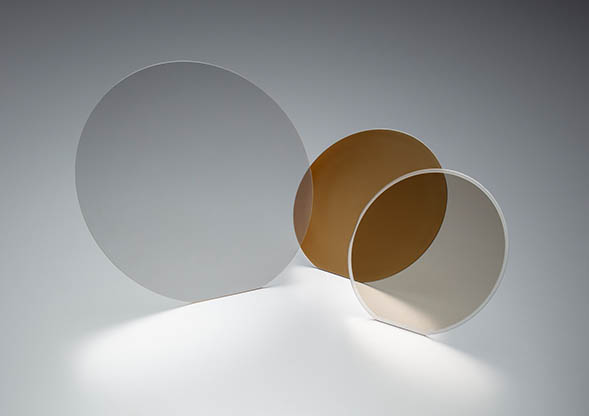
Created using NGK’s proprietary liquid phase crystal growth method, the gallium nitride (GaN) wafer exhibits low dislocation density across the entire wafer surface.
We have developed two different types of GaN wafers: a semi-insulating type for high frequency devices for 5G and 6G wireless base stations; and a conductive type for the power devices incorporated into electric vehicles (EVs), power control units, and optical devices used as light sources for projectors.
Properties
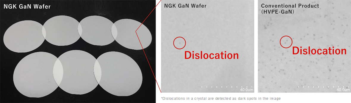
Realizes high crystallinity
GaN wafers crystallized from a liquid-phase equilibrium system exhibit remarkably high crystallinity, with few dislocations.
In addition to improving reliability, high crystallinity helps increase the output and efficiency of optical devices, RF devices, and power devices manufactured using these wafers.
Cathodoluminescence image*
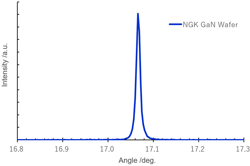
X-ray rocking curve measurement*
| Diffraction plane | FWHM |
|---|---|
| (0002) | 50 arcsec.(typical) |
- *Crystalline quality is evaluated by sharpness of diffraction X-rays.
Specifications
| Item | Unit | 2-inch | 4-inch | 6-inch |
|---|---|---|---|---|
| Diameter | mm | 50 ± 0.3 | 100 ± 0.3 | 150 ± 0.3 |
| Thickness | µm | 330 ± 30 | 360 ± 40 | 400 ± 60 |
| TTV | µm | ≦ 20 | ≦ 20 | ≦ 50 |
| SORI | µm | ≦ 25 | ≦ 50 | ≦ 100 |
| Surface orientation | - | (0001) | (0001) | (0001) |
| Off-angle | degree | 0.5 ± 0.2 | 0.5 ± 0.25 | 0.5 ± 0.3 |
| Dislocation density | /cm2 | ≦ 2x10⁶ | ← | ← |
| Resistivity (conductive) | Ω・cm | ≦ 0.02 | ← | ← |
| Resistivity (semi-insulating) | Ω・cm | ≧105 | ← | ← |
| Gallium-face | - | Polished and surface treatment | ← | ← |
| Nitrogen-face | - | Lapped and etched | ← | ← |
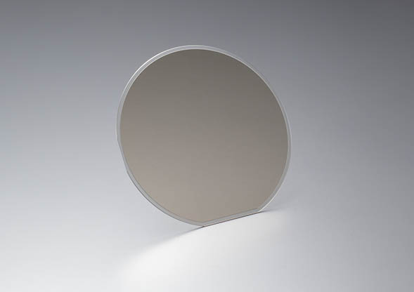
Newly Developed Bonded Semi-Insulating GaN Wafer
This new product features lower dislocation density and higher heat dissipation performance than current products, thereby contributing to improved GaN device performance.
NGK has developed a novel bonded semi-insulating GaN wafer that combines a GaN thin film with a silicon carbide (SiC) base substrate. Adding the high heat dissipation of the SiC to the low dislocation density of the GaN wafer should enhance the performance of high frequency devices at lower cost.

Inquiry about Research & Developments
Please apply with the contact form and give us your comments or questions.