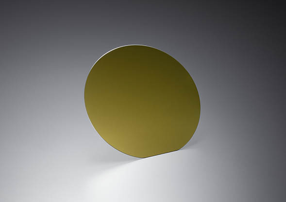
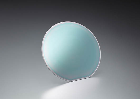
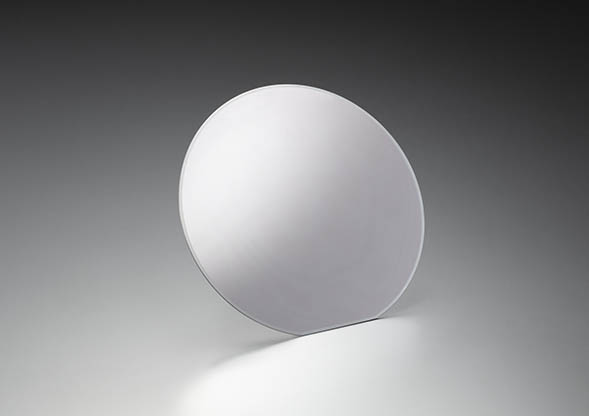
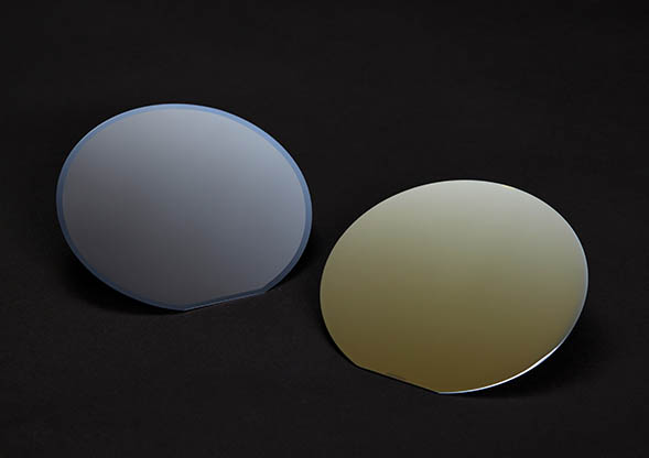
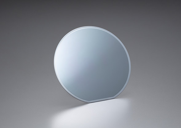
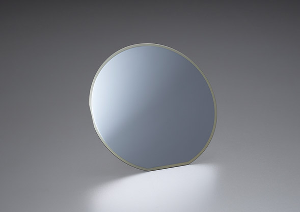
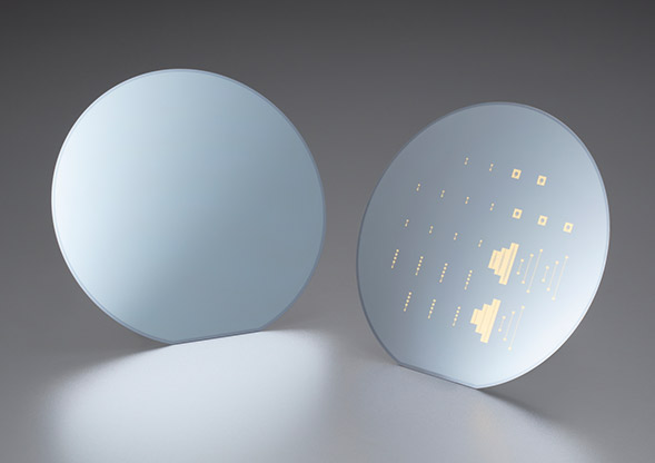
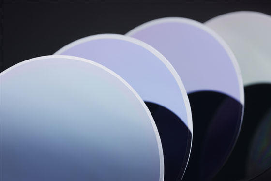
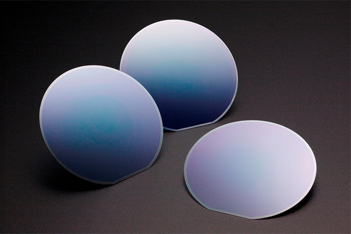
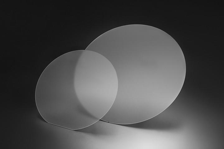
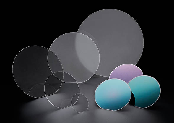
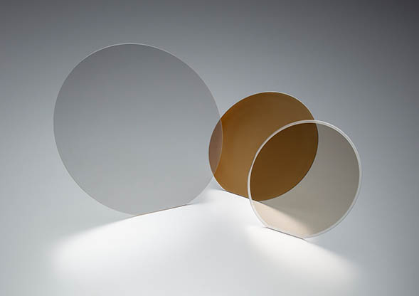
Creating new products

Next-generation wafers, intended for ultra-high-speed communications and EV power devices

Overview of products under development

Next-generation wafers

High-speed wireless communication networks like 5G and 6G require power amplifiers and filters capable of operating at higher frequencies. Data centers and core/metro networks require optical devices capable of handling optical transmissions at ultra-high-speed and with low power consumption. Beyond this, demands for higher output power, lower power loss, and greater reliability are expected to emerge for devices used in electric vehicles (EVs) and other applications.

To offer solutions that meet these all needs, NGK is currently developing high-performance next-generation wafer products that draw on our proprietary crystal growth method, ultra-precision-polishing technology, and multi-materials bonding technology.

Wafer products under development

Aluminum Nitride (AlN) Wafer

AlN wafers improve the performance of the deep ultraviolet light-emitting diodes (UVC-LEDs) used for sterilization. These wafers are also expected to find applications in next-generation power semiconductors. Using proprietary manufacturing methods, we have succeeded in producing 4-inch single-crystal AlN wafers, production in large diameters of which was previously regarded as difficult.

Photo from left to right: A 2-inch and 4-inch wafer

TFLN bonded wafer for optical communications

TFLN bonded wafers for optical communications are high-performance wafers made by precision-polishing a bonded wafer consisting of lithium niobate (LN/ LiNbO3) bonded to a base substrate. This product offers thin-film LNs free of crystal damage, which contributes to the development of optical modulation devices featuring lower power consumption and smaller dimensions—ideal for data centers and core/metro networks.

Photo shows a 6-inch wafer

LT/LN bonded wafer for wireless communications

LT/LN bonded wafers for wireless communications are wafers used for SAW filters, made of lithium tantalate (LT/ LiTaO3) and lithium niobate (LN/ LiNbO3). NGK is currently manufacturing these wafers while also developing new ones by refining its proprietary direct-bonding and precision-polishing technologies to create high-frequency filters for 5G and 6G communications.

Photo shows a 6-inch wafer

PZT bonded wafer for MEMS devices

These bonded wafers are made by sintering high-performance PZT—a material that physically deforms upon electrical stimulation and generates electricity when physically deformed—which is bonded to various base substrates at room temperature. The wafers are precision-polished to a thickness of 10 to 50 μm. The larger displacements that can be achieved in this way compared to conventional film-deposited wafers allows the production of high-performance actuators and high-sensitivity sensor devices.

SiC bonded wafers for optics

SiC bonded wafers for optics consist of SiC, SiO2 and Si. SiC is difficult to thin, but the wafers can be realized by NGK's state- of- arts precision polishing process.
SiC has a large non-linear optical co-efficient and a large band gap, so it can be used in wide wavelength range such as visible light to infrared light as wavelength conversion devices and wide wavelength bandwidth light sources, and is expected to be applied to data centers, quantum computers and quantum communications.

Photo shows a 4-inch wafer

InP bonded wafers for high-power lasers

InP bonded wafers for high-power lasers are manufactured by directly bonding InP and SiC, a high heat-dissipating material.
NGK proprietary bonding and polishing technologies can suppress the heat generated by lasers formed on InP wafers, and are expected to be applied to high-power lasers for telecoms and laser light sources with built-in high-speed optical modulators for AI servers.

Photo shows a 4-inch wafer

Quartz glass bonded wafers for sub-THz wireless communication

Quartz glass bonded wafers are manufactured by directly bonding quartz glass and silicon. Quartz glass provides low loss performance against sub-THz waves, and Si has relatively high heat dissipation properties. It contributes to the realization of antenna circuit boards with low loss, wide frequency bandwidth, high heat dissipation performance and high reliability for 6G communications and high frequency radar.

Photo shows 4-inch wafers

Related products

Inquiry about Research & Developments

Please apply with the contact form and give us your comments or questions.

Contact